From the number of emails I receive and posts on various digital camera user groups, it seems that many digital camera users still don't know how the primary function of their camera works. It doesn't help to have representatives from camera companies over the years:
- make untrue claims ("Our camera doesn't interpolate, you get the real pixels")
- obscure details in marketing claims ("Our camera produces 12.1 effective megapixels")
- fail to understand basic optic theory ("The smaller sensor size produces 1.5x magnification, making all your lenses longer in focal length")
- make misleading statements about competitors ("They use a CMOS sensor, which is noisier than a CCD sensor")
- make misleading statements about themselves ("Our sensor doesn't produce moire because it isn't a Bayer pattern")
- make claims that most people don't have the knowledge to interpret correctly ("Industry leading 88db signal-to-noise ratio")
The list is seemingly endless. (And yes, all those claims were historically made by a camera maker.)
It's important to understand how sensors function if you want to get the best possible results from your camera. So I'll step you through what happens, and the issues associated with a number of practical problems you'll encounter.
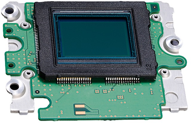
A camera focuses light on a plane behind the rear element of the lens. In 35mm cameras, that plane contains film. In digital cameras, the plane is occupied by a piece of silicon (chip) which I'll refer to as the sensor. Sensors historically have come in two primary types: CCD (charge-coupled device) and CMOS (complimentary metal oxide).
A few words about CCD versus CMOS before we continue:
- CCD is an older technology that is now mostly abandoned. CCD sensors are easy to design and produce. But virtually all camera makers moved away from CCD for a variety of reasons, though, as the advantages of CCD became outclassed by what engineers can do with CMOS. CCD does have the advantage of using line or frame transfers, the latter of which has some temporal advantages for video. CCD sensors have more tendency towards blooming (letting electrons escape from one location to a neighboring one). Again, CCD is a mature technology. Most of the major advances we've seen in CCD tech occurred long ago.
- CMOS has the advantage of often being less expensive to manufacture in quantity, but more importantly CMOS sensors are able to contain more complex internal electronics at each individual sensing area (called a photosite) as well as adjacent to the image area. The latest CMOS sensors—for example the Sony EXMORs—have on-board analog-to-digital converters with exceedingly low read noise and a very large dynamic range. In general it takes more money and a longer time to design a CMOS sensor, but in the end you get the advantage of lower cost and higher capability.
Long term, CMOS is the foundation of all camera image sensors. But CMOS does have some issues. One is that you need very fast support circuitry on the chip in order to avoid issues such as rolling shutter.
Because CMOS addresses pixels directly, most CMOS sensors don't capture a "frame" of video simultaneously and offload that to external circuity. Instead, rows of pixels are read sequentially, meaning the top of the frame occurs ever so slightly sooner than the bottom of the frame in video captures. While the sensor makers can improve that speed, that introduces electronic noise with current technologies.
Nikon at one point showed a variation in sensor design: a CMOS variant that uses a different transistor type (the LBCAST sensor used in the D2h and D2hs). While we don't talk about "buried" channels any more, which was the LBCAST advantage, most current CMOS sensors inherit pretty much all of the innovations that came about earlier, such as some form of LBCAST. We will continue to see a stream of new acronyms as technology and material use moves inexorably on in the low levels of each sensor.
On the other hand, some terminology used around image sensors is faux info: the so-called LiveMOS sensors used in m4/3 cameras are really nothing more than CMOS with a fancy marketing name.
At present, virtually all of the camera image sensors you'll encounter are CMOS and come from either Canon or Sony (with the latter, sometimes companies make additional changes to something Sony Semiconductor produces). CMOSIS and TowerJazz produce a few sensors that are used by a couple of makers, as well. But by and large, you're likely to be using a camera whose image sensor was created on a Canon or Sony fab (manufacturing plant that produces semiconductors).
On an image sensor you’ll find an array of light-sensitive spots, called photosites. Photosites are usually square in shape (there have been two major exceptions that I'll deal with in a moment), and laid out in rows and columns.
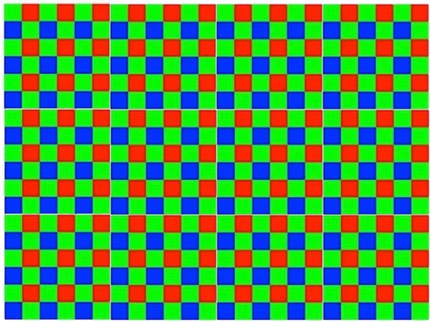
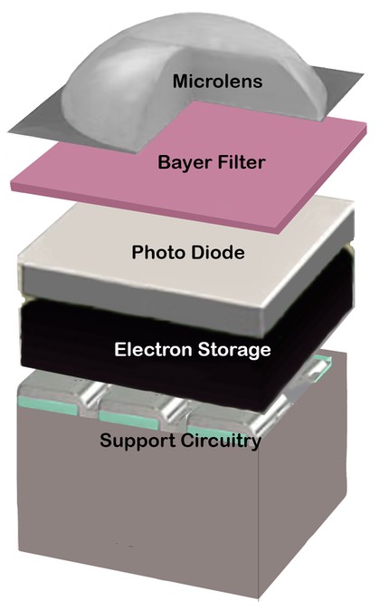
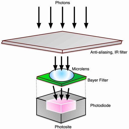
The first thing that catches newcomers to digital cameras unaware is this: the light-sensing portion of the photosites—called the photo diode—does not necessarily cover the entire surface area of the sensor on a front-illuminated sensor (FSI). With some older sensors the active light gathering area has been as little as 25% of the total surface area of the chip (called the "fill factor"). Yes, that means that there can be non-light responsive space between adjacent photo diodes. (Pictures or representations that show adjacent red, blue and green photosite positions, like the one above, are usually of an array of microlenses and filters that lie on top of the actual sensor, and not the photosite and embedded photo diode.)
In recent times we've had BSI (backside illuminated) sensors (above illustration), where the fill factor is basically 100%, as the light photons don't have to go down deep into the sensor to be captured and stored as charge. BSI and it's 100% fill factor generally is most useful on smaller sensors (phones, compact cameras), as large sensors such as full frame already have a large fill factor. We don’t see BSI as often on large sensor cameras (DSLRs), and when we do, it usually is for another aspect of BSI design (typically faster and more support circuitry that doesn't interact as much with the photo diode.
I noted that there have been exceptions to the square photosite rule. The most important ones for DSLR users were:
- The Nikon D1x. The D1x has two adjacent photosites that were binned (combined) on the column axis, which created a final photosite that was rectangular.
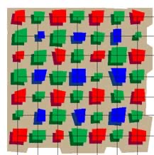
- The Fujifilm SuperCCD (used in the Fujifilm S1, S2, S3, and S5 bodies). The SuperCCD uses quasi-octagonal photosites. Fuji further places the "grid" for the photosites at an angle, though for all practical purposes it still has rows and columns of photosites, just oriented at a 45 degree angle.
You might wonder just how large the individual photosites are. On the original D1, they were 11.8 microns square, which is quite large (though technically, this was a group of four "binned" photosites that worked together). On the old Coolpix 990, they were 3.45 microns square, which was considered small when that camera appeared in the late 90’s, but would be considered large for current compact cameras.
The tendency has been towards smaller photosites, partly because photo diode efficiencies have gotten better. Thus, current DSLRs tend to have photosites in the 4 to 8 micron square range, while current compact cameras like the Coolpix can have photosites as small as about 2 microns square (some camera phones have even smaller photosites, ranging down to 0.9 microns).
Note that it's the overall area of a photosite that's important. A 3 micron photosite has 9 square microns of area (of which only a portion may be sensitive to light if it’s not BSI). An 8 micron photosite has 64 square microns of area, or almost an order of magnitude more area. That turns out to be fairly important, as photons are random, so the larger the area you collect photons over, the less "shot noise" there will be.
Dark Current and Well Overflow
A photosite essentially converts the energy from a light wave into photo-electrons. Light is actually what physicists call a "wave-particle duality." The energy in the light, which is what we're trying to collect, resides in particles called photons. The longer a photosite is exposed to light, the more photons are converted into photo-electrons via the photo diode at each photosite. One photon = one photo-electron maximum (you can't gain energy in the transfer in current sensor designs). To some degree, photo diode size is directly related to effective ISO sensitivity, as a larger surface area exposes it to more light in any given amount of time than a smaller surface would. You'll note that the larger photosite DSLRs tend to have base ISOs of 200 and the smaller photosite DSLRs tend to have a base ISO of 100, for example.
The physical size of the individual photosites is important beyond effective ISO. The larger the active light gathering surface, the less certain types of noise can be a problem. That's because every piece of silicon has a baseline level of electron "action" (current). In sensors, this current is usually called Dark Current or Dark Noise (the "dark" in the name implies that the current was formed despite no exposure to light). (There are actually several different underlying types of on-chip noise, but for simplification, I'll just refer to Dark Current in this article.)
Dark Current increases with temperature. This is due to the small gap between the valence and conduction bands within the silicon: the gap is so small that higher temperatures cause more electrons to cross the gap to where they don't belong. Fortunately, it takes really hot temperatures to increase Dark Current to visible, troublesome noise (typically 90 degrees Fahrenheit or higher coupled with long shutter speeds, at least for the Canon and Sony sensors used in most cameras). At very long shutter speeds (usually 1 second or longer) some of this electron activity can also result in "hot pixels," essentially generated by photosites that prove "sticky" to those wandering electrons due to impurities in the silicon. The longer the shutter speed or higher the temperature, the more likely you'll see some hot pixels in your image.
Every digital camera attempts to deal with dark current by "masking off" a small set of photosites so that they don't see light (which is part of the explanation why your supposedly 25.28-megapixel camera only produces images with only 24.5 megapixels). Your camera's electronics compares the values it sees from photosites that weren't exposed to light to those that were. Dark Current is partially random. So, in the most simplistic form, the camera averages all the values found in the masked off photosites and subtracts that from the values seen by the photosites exposed to light to remove the Dark Current. Fortunately, better algorithms have been developed over the years, and some sensors are quite good at using this masked area to remove underlying noise.
Many current production digital cameras go further than that, however. Individual photosites can and do have slightly different responses to light and to current, so many modern cameras do something a bit different on long exposures: they take two pictures with the photosite array, one exposed to light and one not (usually called Long Exposure Noise Reduction). Then the pattern seen in the exposure without light is subtracted from the one for the exposure exposed to light.
(You can do this yourself, by the way. When you take a picture in low light with long shutter speeds, especially in warmer temperatures, put the lens cap on and take another shot at exactly the same shutter speed. In Photoshop you can use the second exposure to remove patterned noise from the first. But make sure that your dark current exposure is taken at the same temperature as the first! I've seen people take their first photo outside at night in the cold, then bring the camera to the warmer indoors while the second dark current exposure is being made. That won't work: the two exposures need to be done at the same temperature.)
At the other end of the spectrum, what happens to a photosite when it contains too many photo-electrons (due to too much exposure to light)? Well, if left to its own devices, the information (electrons) can spill from one photosite to another, corrupting the data in the adjacent site (a concept called "blooming," or well overflow). This is especially true in the physically small photosites of the Sony CCD sensors used in older compact camera models (proximity makes it easier for an electron to escape from its current owner to another). Most sensors have "drain" circuits that attempt to remove excess electrons before they degrade the chip's data too badly, but these circuits are far from perfect, and it's possible to overload them, as well.
I've been writing about something without really identifying it: the "electron well" coupled to a photosite. The photo diode in the photosite converts the light photons to a charge (electrons), but the photosite needs somewhere to store that charge until the sensor is asked to produce the "value" for each photosite. It does this in an electron well typically buried under the photosite these days (in very old sensors, it was sometimes adjacent). Just like the size of the photo diode varies in sensors, so does the size of the electron well. Compact cameras have smaller wells than DSLRs, for example.
Let's just use some arbitrary numbers to see why that's important.
Consider a compact camera photosite well that can hold 10,000 electrons versus a DSLR well that can hold 100,000 electrons. If the baseline noise level of the electronics within the sensor itself is 100 electrons, then the signal to noise ratio in the compact camera has a maximum value of 100:1 while the DSLR's signal to noise ratio is 10 times better. That's just one reason why the compact cameras produce more noise—all else equal—than do DSLRs.
Sensor design is old enough now that we're bumping against some physical limits in almost all the areas just mentioned:
- Photo diodes are getting to be about the maximum size they can be within the photosite without some new technological breakthrough.
- Both BSI and microlens technology means that all the possible light gets into the photo diode (e.g. 100% fill factor).
- Baseline noise is now about as low as can be mass produced with current materials in current image sensors.
- Electron well sizes are about maximized for the current photosite sizes.
You can make some adjustment to one of those variables, but it tends to make you have to reduce one of the other variables. Thus, we currently see much more emphasis on post processing the sensor data produced and getting cleaner results by taking out problems after the fact.
However, that doesn't mean we're done with breakthroughs, only that it takes a complete rethink of an element to make significant progress. One such thing is to reverse the orientation of the photo diode so that it's on the surface rather than buried further down in the silicon (sometimes called a "backlit sensor", or more commonly referred to as BSI). Different materials—often more expensive and more difficult to work with—can change the baseline responses. Better microlenses and filtration can get more of the original light to the photo diode itself. We still have room for some improvement, and I think we'll continue to see a same level of improvements over the next few years that we saw in the previous few. Further out than that is difficult to predict, as it would take some new breakthrough technologies to make a large improvement rather than an incremental one.
Your Digital Camera Sees in Monochrome
It may surprise you to find out that the sensor in your camera reacts to all light with relative equality. Each individual photosite simply collects only the amount of light hitting it and passes that data on; no color information is collected. Thus, a bare sensor is a monochromatic device.
Plenty of ways exist to make monochromatic information into color data. For example, you could split the light coming through the lens to three different sensors, each of which was tuned to react to a certain light spectrum (some video cameras do that). But most digital still cameras use a different method: they place an array of colored filters over the photosites. One filter arrays is commonly used, and several others are possible:
- RGBG (Bayer). This array arrangement usually involves odd-numbered rows of photosites covered by alternating red and green filters, with even-numbered rows covered by alternating green and blue filters. Called the Bayer pattern after the Kodak engineer that invented it, this filter array uses the primary colors of the additive mixing method (used in television and computer monitors). One unique aspect of the Bayer pattern is that each "color" cell has two of each of the alternatives as its neighbors. Most current digital cameras use a Bayer pattern array. This is the method used in all current Canon and Nikon DSLRs.
- Diagonal color. One common alternative Bayer arrangement, called the diagonal color pattern, is where each row has repeating RGB elements and each row is staggered by one element (i.e., the first row is RGBRGBRGB..., the second row is GBRGRBRBR..., the third row is BRGBRGBRG...), but it is not currently used in any digital camera. The Fujifilm mirrorless cameras using the X-Trans technology use a relative of this pattern that has less color information than luminance, but it's not exactly a diagonal pattern.
- Add a Color. There are some very sophisticated patterns of R, G, and B filtration where the second green is replaced by something else. Sony tried emerald, and Kodak had a version with no filtration on that fourth position. You need fairly high pixel counts to mask the low-level artifacts caused by these patterns, but you can tune them for either color discrimination or luminance gathering.
- CYMG. Alternatively, a slightly more complex filter array related to both Bayer uses the primary colors in the subtractive process (commonly used in printing technologies) plus green. This was the method used in most early Coolpix models beginning with the 900 series (i.e., the 885, 995, 2500, 4500, 5000, and 5700 all use this pattern). CYMG is typically used on sensors that are sensitive to noise at low light levels, as the dyes used to create the CYM colors are lighter than RGB and thus let more light through to hit the photosites. However, color discrimination is a little tougher to do with CYMG than it is with RGB.
Each of these methods has advantages and disadvantages. The repeat of the green filter in Bayer patterns (and addition of a green filter to the subtractive CYM method) is due partly to the fact that our eyes are most sensitive to small changes in green wavelengths. By repeating (or adding) this color in the filter, the accuracy of the luminance data in the critical area where our eyes are most sensitive is slightly improved.
So, each individual photosite has a filter above that limits the spectrum of light it sees. Later in the picture-taking process, the camera integrates the various color information into full-color data for individual pixels (a process sometimes called interpolation, but more accurately called demosaicing).
But one important point should be made: the color accuracy of your digital camera is significantly influenced by the quality of the filter array that sits on top of the photosites. Imagine, for a moment, a filter array where each red filter was slightly different—you'd have random information in the red channel of your resulting image. A damaged filter would result in inaccurate color information at the damage point.
One thing that isn't immediately apparent about the Bayer pattern filter is that the ultimate resolution of color boundaries varies. Consider a diagonal boundary between a pure red and a pure black object in a scene. Black is defined as the absence of light reaching the sensor, thus the data value would be 0 (for the G and B photosites). That means that only the photosites under the red sensors are getting any useful information! Fortunately, pure red/black and blue/black transitions don't occur as often as you'd think, but it is something to watch out for. (Since no individual color is repeated in a CYMG pattern, all boundaries should render the same, regardless of colors.)
Most sensors these days are built with microlenses that incorporate the filter pattern below them and sit directly on top of the photosites. This microlens layer not only incorporates the Bayer filter pattern just underneath it, but redirects light rays that hit at an angle to move more perpendicular to the photosites. If light were to hit the photosites at severe angles, not only would the photosite be less likely to get an accurate count of the light hitting it, but adjacent cells would tend to be slightly more influenced by the energy since the filters sit above the photosites and have no "guards" between them. All Nikon cameras currently use microlens layers; the old Kodak DCS Pro 14n is unusual in that it didn't.
On top of the microlenses are yet another set of filters that take out the ultraviolet (UV) and infrared (IR) light spectrum and provide anti-aliasing (I'll discuss anti-aliasing in the next section). Current cameras allow very little light outside the visible spectrum to get to the photosites, though many older ones often let significant IR through.
We have one more exception to talk about (sensors have gotten complicated since I first wrote about them in the 1990's). That's the Foveon sensor (now owned by Sigma, the only cameras that use it). Unlike the Bayer-pattern sensors that get their color information by using adjacent photosites tuned to different spectrums, the Foveon sensor uses layers in its photosite design. The primary benefit of this approach is that it gets rid of color aliasing issues that occur when you demosaic Bayer-pattern data, and thus allows you to get rid of (or at least lower the value of) the antialiasing filter over the sensor. The benefit can be described in two words: edge acuity. Another benefit is that there is no guessing about color at any final pixel point, which means that colors are generally robust and, with a lot of intense calculation, accurate. The primary disadvantage to the Foveon approach is noise. Obviously, less light gets to the bottom layer of silicon in a photosite than the top layer. Foveon has done a remarkably good job of mitigating the drawbacks while emphasizing the positive in the latest iteration of the sensor.
Getting Data Off the Sensor
At this point, we have an array of filtered photosites that respond to different colored light that usually looks something like this:
The data at each of the individual photosites, by the way, is still in analog form (the number of electrons in the well). The method by which that data is retrieved may surprise you, however: in most CCD sensors the values are rapidly shifted one line at a time to the edge of the sensor. This process is called an interline (or row) transfer, and the pathways that the data moves down are one of the reasons why photosites on CCDs have space between them (to make room for the pathway). While the data is moved off in "rows," it's important to note the short axis is usually the direction that the data is moved (if you're looking at a horizontal image, you'd see these as columns). CMOS sensors, such as those used in all recent Canon and Nikon DSLRs, are unique in that the data for each individual sensor can be retrieved directly, though this is generally also done in columns on most CMOS sensors.
As the data moves to the edge of the sensor, it is usually first correlated to reduce noise, then read by analog to digital converters (ADC). From the ADC get a series of digital values, typically called Digital Numbers (8-bit for many Coolpix and consumer cameras, 12-bit to 16-bit for most SLR models). On most recent CMOS designs (starting with the Nikon D90/D300, for example), the ADC function is actually built into the image sensor rather than a separate circuit off the sensor. This reduces "read noise" as transmission errors don't come into play.
One common misconception is that bit depth equates to dynamic range (the range of dark to bright light that can be captured). This isn't true. Dynamic range of a camera is determined mostly by the sensor (electron well capacity minus baseline noise determines the maximum range of exposure tolerated; another reason why larger photosites are better than small). If you were to put a 4-bit, 8-bit, 12-bit, and 16-bit A/D converter on the same chip, the photo diode of the sensor wouldn't respond to low or bright levels of light any differently; you'd only get more or less tonal definition in the analog-to-digital conversion. In essence, you get more precise Digital Numbers with more bits, less precise with fewer bits, but the underlying data is the same.
Demosaic
At this point in a Bayer sensor, we have one-third the data we need for a complete color picture (we need red, green, and blue values at each photosite location, and we have only one of those values from each photosite). Here comes the tricky part: a processor (a Sparc-based computer in many early Coolpix models, dedicated proprietary circuits in most new cameras, called the EXPEED engine by Nikon, DIGIC by Canon, BIONZ by Sony, all of which use ARM central processors these days) looks at blocks of this data and tries to guess the actual RGB color value of each pixel by comparing adjacencies! The demosaicing I mentioned above.
A simple demosaicing routine might work this way:
- Record the existing R, G, or B value at each pixel position
- Invent new G values at each of the R and B photosite positions, often using a multiple pass technique to figure out where edges occur
- fill in the missing R and B values using neighbor sampling techniques.
That's a gross simplification. Hundreds of more sophisticated variants are now used, with most trying to deal with the artifact issues created by the simpler routines.
Camera manufacturers are extremely secretive about their demosaicing methods. But given the unclassified data on image processing and the fact that virtually all cameras are pressed for computational power when confronted with huge amounts of data, they all tend to do similar things with near-neighbor lookups. You should know a couple of things about demosaicing (we're about to talk about anti-aliasing, which I promised earlier).
The process of reconstructing data at a "frequency" (digital sampling rate) less than the original (which is analog) produces aliasing. What that means is that the reconstructed data may not be a correct record of the original.
Let's pretend our sensor is black and white only for a moment. Imagine a series of vertical black lines with white space between them. If each black line fell on one column of photosites and each white space fell on the column of photosites next to it, it should be obvious that we can capture that level of detail perfectly.
But what happens if each black line falls partially on a second column of photosites? Instead of recording white, those photosites would record "gray" (part white, part black).
Earlier I mentioned that the filter on top of the microlens Bayer pattern took out IR and provided anti-aliasing. Well, what anti-aliasing filtration does is get rid of the highest frequency detail, which would tend to produce the problems we just talked about. Unfortunately, anti-aliasing filters have the net effect of making the level of detail rendered appear "softer" than they would otherwise. But they also insure that the worst artifacts associated with analog-to-digital sampling aren't encoded into the Bayer pattern data.
The higher the resolution of the sensor, the less the need for anti-aliasing filtration; the 45mp D850 doesn't have an anti-aliasing filter, for instance. Technically, the D6 shouldn't need one, but it does have a mild one. Nikon gave us the option on the original 36mp D800 and D800E pair (as did Canon with their later 5DS/R pair). These days, sensors with high pixel density (20mp+ for APS-C, 36mp+ for full frame) tend to not use anti-aliasing filtration.
One of the artifacts associated with sampling frequency and demosaicing is that of moire patterns (sometimes called color noise). A moire pattern occurs when aliasing occurs on a highly detailed area. Moire can be partially removed by using complex math (involving what's known as the Nyquist frequency), but there's a real battle going on inside your digital camera between the speed at which images are processed and the amount of data the camera has to deal with. Most cameras saving into JPEG format don't do much, if any, moire processing, and rely more upon the anti-aliasing filter to reduce this artifact before the data is encoded. Again, some high-pixel density cameras, the D850 for example, don't use an anti-aliasing filter. Images from those cameras tend to be slightly "sharper" and contain slightly more detail than others of the same pixel count, but this is at the expense of possible added color noise and stairstep artifacts.
Sharpness, contrast, and other camera settings may be applied during the demosaicing step or immediately afterwards, depending upon the camera's design. And JPEG compression is yet another variable that enters into the picture. Each additional manipulation of the underlying photosite data gets us a little further from the original information and introduces the potential for artifacts. In essence, by the time the camera is done with all its processing, it is impossible to reconstruct the original data (exception: most modern DSLR cameras have the ability to save the actual photosite data from the camera in a raw file, for later demosaic on your computer).
Those using older DSLRs should know a couple of things about a few cameras:
- On Fujifilm's Web site, they make the contention that their SuperCCD does not interpolate to get the 6-megapixels of data the S1 produces from its 3-megapixel sensor (or 12 megapixels from 6 on the S2 Pro, S3 Pro, or S5 Pro). They claim that, because of the angular nature of their array (think of a baseball diamond where each of the bases is a photosite), that they already have the X and Y values that can be used to build the intermediaries (the pitcher's mound in this pattern). Sorry, Fujifilm, but that's still interpolation.
- The D1x is a very unique camera as regards demosaicing. Most interpolation of photosite data is what is called up sampling. This means that you sample existing data to produce additional data (that's what demosaicing does, for example: you have a G value and you look at the other data around it to come up with the R and B values for that G position). You can also down sample, which would be to produce less data than the original contains. The D1x upsamples the short axis and downsamples the long axis to produce its in-camera pictures. NEF conversion products, such as the no-longer made Bibble and versions of Capture later than 3.5, can also produce images that don't downsample the long axis while upsampling the short axis, producing far larger files.) Why Nikon chose to do the in-camera up/down sampling is unclear. One would think that you wouldn't want to downsample sensor data normally, but the fact that Nikon does so even in their default RAW processing seems to indicate that Nikon knows something about the validity of the data from those split photosites that we don't. It could be, for example, that Nikon downsamples that data to deal with a noise issue. Or it could be that there's a short-cut to the number-crunching that must done to generate the full RGB image if they downsample the long axis. The reason must be a good one, however, because moire and related artifacting is dramatically lessoned if sampling is done on only one axis rather than two.